
Transparent Display Technology
1. History OF OLED
The first
observations of electroluminescence in organic materials were in the early
1950s by A. Bernanose and co-workers at the Nancy-Université, France. They
applied high-voltage alternating current (AC) fields in air to materials such
as acridine orange, either deposited on or dissolved in cellulose or cellophane
thin films. The proposed mechanism was either direct excitation of the dye
molecules or excitation of electrons.
In 1960, Martin
Pope and co-workers at New York University developed ohmic dark-injecting
electrode contacts to organic crystals. They further described the necessary
energetic requirements (work functions) for hole and electron injecting
electrode contacts. These contacts are the basis of charge injection in all
modern OLED devices. Pope's group also first observed direct current (DC)
electroluminescence under vacuum on a pure single crystal of anthracene and on
anthracene crystals doped with tetracene in 1963using a small area silver
electrode at 400V. The proposed mechanism was field-accelerated electron
excitation of molecular fluorescence.
Pope's group
reported in 1965 that in the absence of an external electric field, the electroluminescence
in anthracene crystals is caused by the recombination of a thermalized electron
and hole, and that the conducting level of anthracene is higher in energy than
the exciton energy level. Also in 1965, W. Helfrich and W. G. Schneider of the
National Research Council in Canada produced double injection recombination
electroluminescence for the first time in an anthracene single crystal using
hole and electron injecting electrodes,the forerunner of modern double
injection devices. In the same year, Dow Chemical researchers patented a method
of preparing electroluminescent cells using high voltage (500–1500 V) AC-driven
(100–3000 Hz) electrically-insulated one millimetre thin layers of a
melted phosphor consisting of ground anthracene powder, tetracene, and graphite
powder.[ Their proposed mechanism involved electronic excitation at
the contacts between the graphite particles and the anthracene molecules.
Device
performance was limited by the poor electrical conductivity of contemporary
organic materials. This was overcome by the discovery and development of highly
conductive polymers.For more on the history of such materials, see conductive
polymers.
Electroluminescence
from polymer films was first observed by Roger Partridge at the National Physical
Laboratory in the United Kingdom. The device consisted of a film of
poly(n-vinylcarbazole) up to 2.2 micrometres thick located between two charge
injecting electrodes. The results of the project were patented in 1975 and
published in 1983.
The first diode
device was reported at Eastman Kodak by Ching W. Tang and Steven Van Slyke in
1987.This device used a novel two-layer structure with separate hole
transporting and electron transporting layers such that recombination and light
emission occurred in the middle of the organic layer. This resulted in a
reduction in operating voltage and improvements in efficiency and led to the
current era of OLED research and device production.
Research into
polymer electroluminescence culminated in 1990 with J. H. Burroughes et al. at the Cavendish Laboratory in
Cambridge reporting a high efficiency green light-emitting polymer based device
using 100 nm thick films of poly(p-phenylene vinylene).
2. Organic light-emitting diode (OLDE)
An organic
light emitting diode (OLED) is a light-emitting diode (LED) in
which the emissive electroluminescent layer is a film of organic compounds
which emit light in response to an electric current. This layer of organic
semiconductor material is situated between two electrodes. Generally, at least
one of these electrodes is transparent.
OLEDs are used in television set
screens, computer monitors, small, portable system screens such as mobile
phones and PDAs , watches, advertising,
information, and indication. OLEDs are also used in light sources for space
illumination and in largearea light-emitting elements. Due to their early stage
of development, theytypically emit less light per unit area than inorganic
solid-state based LED point-light sources.
An OLED display functions without a
backlight. Thus, it can display deep black levels and can be thinner and
lighter than liquid crystal displays. In low ambient light conditions such as
dark rooms, an OLED screen can achieve a higher contrast ratio than an LCD
using either cold cathode fluorescent lamps or the more recently developed LED
backlight.
There are two main families of
OLEDs: those based upon small molecules and those employing polymers. Adding
mobile ions to an OLED creates a Light-emitting Electrochemical Cell or LEC,
which has a slightly different mode of operation.
OLED displays can use either
passive-matrix (PMOLED) or active-matrix addressing schemes. Active-matrix
OLEDs (AMOLED) require a thin-film transistor backplane to switch each
individual pixel on or off, and can make higher resolution and larger size
displays possible.

3. Architecture of OLEDs
3.1Substrate
(clear plastic, glass, foil)
The
substrate supports the OLED.
3.2Anode
(transparent)
The
anode removes electrons (adds electron "holes") when a current flows
through the device.
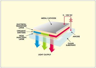
3.3 Organic
layer:
3.3.1Conducting
layer
This
layer is made of organic plastic molecules that transport "holes"
from the anode. One conducting polymer used in OLEDs is polyaniline.
3.3.2 Emissive layer
This layer is made of organic plastic
molecules (different ones from the conducting layer) that transport electrons
from the cathode; this is where light is made. One polymer used in the emissive
layer is polyfluorene.
3.4 Cathode
(may or may not be transparent depending on the type of OLED)
The
cathode injects electrons when a current flows through the device.
4.
AMOLED
Active-matrix OLED (active-matrix organic light-emitting diode )
AMOLED is a display technology for use
in mobile devices and televisions. Oled scribes a specific type of thin
film display technology in which organic compounds form
the electroluminescent material, and active matrix refers
to the technology behind the addressing of pixels.

Active matrix
(AM) OLED displays stack cathode, organic, and anode layers on top of another
layer – or substrate – that contains circuitry. The pixels are defined by the
deposition of the organic material in a continuous, discrete “dot” pattern.
Each pixel is activated directly: A corresponding circuit delivers voltage to
the cathode and anode materials, stimulating the middle organic layer. AM OLED
pixels turn on and off more than three times faster than the speed of
conventional motion picture film – making these displays ideal for fluid,
full-motion video.
5. Technical of AMOLED
Two primary TFT backplane technologies, poly-Silicon (poly-Si) and
amorphous-Silicon (a-Si) are used today in AMOLEDs.

Passive-Matrix
Structure Active Matrix Structure
AMOLED is a display technology for use in mobile devices and
televisions. Oled scribes a specific type of thin film display technology
in which organic compounds form
the electroluminescent material, and active matrix refers
to the technology behind the addressing of pixels.
TFT backplane technology is crucial in the fabrication of
AMOLED displays.
Two primary TFT backplane technologies, namely polycrystalline silicon (poly-Si)
and amorphous silicon (a-Si), are used today in AMOLEDs.
These technologies offer the potential for fabricating the active
matrix backplanes at low temperatures (below 150°C) directly onto flexible
plastic substrates for producing flexible AMOLED displays.
6.
Advantages of AMOLED
6.1 Lower cost in the future:
OLEDs can be printed onto
any suitable substrate by an inkjetprinter or even by screen printing,
theoretically making them cheaper to produce than LCD or plasma displays.
However, fabrication of the OLED substrate is more costly than that of a TFT
LCD, until mass production methods lower cost through scalability. Roll-roll
vapour-deposition methods for organic devices do allow mass production of
thousands of devices per minute for minimal cost, although this technique also
induces problems in that multi-layer devices can be challenging to make.
6.2 Light weight & flexible plastic
substrates:

OLED displays can be
fabricated on flexible plastic substrates leading to the possibility of
flexible organic light-emitting diodes being fabricated or other new
applications such as roll-up displays embedded in fabrics or clothing. As the
substrate used can be flexible such as PET., the displays may be produced
inexpensively.
6.3 Wider viewing angles & brightness: improved
OLEDs can enable a
greater artificial contrast ratio (both dynamic range pixel colours appear
correct and unshifted, even as the viewing angle approaches 90° from normal.and
static, measured in purely dark conditions) and viewing angle compared to LCDs
because OLED pixels directly emit light. OLED
6.4 Better power efficiency:
LCDs filter the light
emitted from a backlight, allowing a small fraction of light through so they
cannot show true black, while an inactive OLED element does not produce light
or consume power.
6.5 Response time:
OLEDs can also have a faster
response time thanstandardLCD screens. Whereas LCD displays are capable of
between 2 and 8 ms response time offering a frame rate of +/-200 Hz, an
OLED can theoretically have less than 0.01 ms response time enabling
100,000 Hz refresh rates.
6.6 High
Perceived Luminance
Perceived
luminance is 1.5 times higher than that of conventional lcd display
6.7 True
Colors
High
color gamut and no color shift by viewing angle and/or gray scales
6.8 Fast
Response
More
vivid and dynamic image quality is realized in moving pictures
7.
Disadvantages of AMOLED
7.1 Current costs:
OLED manufacture
currently requires process steps that make it extremely expensive.
Specifically, it requires the use of Low-Temperature Polysilicon backplanes;
LTPS backplanes in turn require laser annealing from an amorphous silicon
start, so this part of the manufacturing process for AMOLEDs starts with the
process costs of standard LCD, and then adds an expensive, time-consuming process
that cannot currently be used on large-area glass substrates.
7.2 Lifespan:
The biggest technical
problem for OLEDs was the limited lifetime of the organic materials. In
particular, blue OLEDs historically have had a lifetime of around 14,000 hours
to half original brightness (five years at 8 hours a day) when used for
flat-panel displays. This is lower than the typical lifetime of LCD, LED or PDP
technology—each currently rated for about 25,000 – 40,000 hours to half
brightness, depending on manufacturer and model. However, some manufacturers'
displays aim to increase the lifespan of OLED displays, pushing their expected
life past that of LCD displays by improving light out coupling, thus achieving
the same brightness at a lower drive current. In 2007, experimental OLEDs were
created which can sustain 400 cd/m2 of luminance for over
198,000 hours for green OLEDs and 62,000 hours for blue OLEDs.
7.3
Color balance issues:
Additionally, as the OLED
material used to produce blue light degrades significantly more rapidly than
the materials that produce other colors, blue light output will decrease
relative to the other colors of light. This differential color output change
will change the color balance of the display and is much more noticeable than a
decrease in overall luminance.This can be partially avoided by adjusting colour
balance but this may require advanced control circuits and interaction with the
user, which is unacceptable for some users. In order to delay the problem,
manufacturers bias the colour balance towards blue so that the display
initially .
7.4 Efficiency of blue OLEDs:
Improvements to the
efficiency and lifetime of blue OLEDs is vital to the success of OLEDs as
replacements for LCD technology. Considerable research has been invested in
developing blue OLEDs with high external quantum efficiency as well as a deeper
blue color. External quantum efficiency values of 20% and 19% have been
reported for red (625 nm) and green (530 nm) diodes,
respectively.However, blue diodes (430 nm) have only been able to achieve
maximum external quantum efficiencies in the range between 4% to 6%.
7.5 Water damage:
Water can damage the
organic materials of the displays. Therefore, improved sealing processes are
important for practical manufacturing. Water damage may especially limit the
longevity of more flexible displays.
7.6 Outdoor performance:
As an emissive display technology,
OLEDs rely completely upon convertingelectricity to light, unlike most LCDs
which are to some extent reflective; e-ink leads the way in efficiency with ~
33% ambient light reflectivity, enabling the display to be used without any
internal light source. The metallic cathode in an OLED acts as a mirror, with
reflectance approaching 80%, leading to poor readability in bright ambient
light such as outdoors. However, with the proper application of a circular
polarizer and anti-reflective coatings, the diffuse reflectance can be reduced
to less than 0.1%. With 10,000 fc incident illumination (typical test condition
for simulating outdoor illumination), that yields an approximate photopic
contrast of 5:1.
7.7 Power consumption:
While an OLED will
consume around 40% of the power of an LCD displaying an image which is
primarily black, for the majority of images it will consume 60–80% of the power
of an LCD – however it can use over three times as much power to display an
image with a white background such as a document or website. This can lead to
reduced real-world battery life in mobile devices.
7.8 Screen burn-in:
Unlike displays with a
common light source, the brightness of each OLED pixel fades depending on the
content displayed. The varied lifespan of the organic dyes can cause a
discrepancy between red, green, and blue intensity. This leads to image
persistence, also known as burn-in.
7.9 UV sensitivity:
OLED displays can be
damaged by prolonged exposure to UV light. The most pronounced example of this
can be seen with a near UV laser (such as a Bluray pointer) and can damage the
display almost instantly with more than 20 mW leading to dim or dead spots
where the beam is focused. This is usually avoided by installing a UV blocking
filter over the panel and this can easily be seen as a clear plastic layer on
the glass. Removal of this filter can lead to severe damage and an unusable
display after only a few months of room light exposure.
8. Applications of AMOLEDs
1.
TVs
2.
Cell Phone screens
3.
Computer Screens
4.
Keyboards (Optimus Maximus)
5.
Lights
6.
Portable Divice displays
8.1 AMOLED Televisions
Sony
·
Released XEL-1 in February
2009.
·
First OLED TV sold in stores.
·
11'' screen, 3mm thin
·
$2,500 MSRP
·
Weighs approximately 1.9 kg
·
Wide 178 degree viewing angle
·
1,000,000:1 Contrast ratio
8.2 Optimum Maximums Keyboard
•
Small
OLED screen on every key
•
113 OLED screens total
•
Each key can be programmed to preform a series of
functions
•
Keys can be linked to applications
•
Display notes, numerals, special symbols, HTML codes,
etc...
•
SD card slot for
•
storing
settings
9. Future Uses for AMOLED
9.1 Lightin
•
Flexible / bendable lighting
•
Wallpaper lighting defining new ways to light a space
•
Transparent lighting doubles as a window
9.2 Cell Phones
•
Nokia 888
9.3Transparent Car Navigation System on Windshield
•
Using Samsungs' transparent AMOLED technology
•
Heads up display
•
GPS system
9.4 Scroll Laptop
•
Nokia concept AMOLED Laptop


